
Applications Powered
by YURAY
Enabling innovation across semiconductor, photonics, sensing, and emerging high-performance applications
High-density interconnects for advanced chip packaging.
Vertical silicon interconnects for heterogeneous integration.
Glass-based vertical interconnects for advanced packaging.
Precision metal deposition for semiconductor interconnects.
Reliable wafer/glass bonding for 3D integration.
Thin-film deposition for advanced semiconductor manufacturing.
Microfabrication &
Advanced Packaging
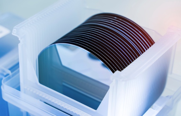
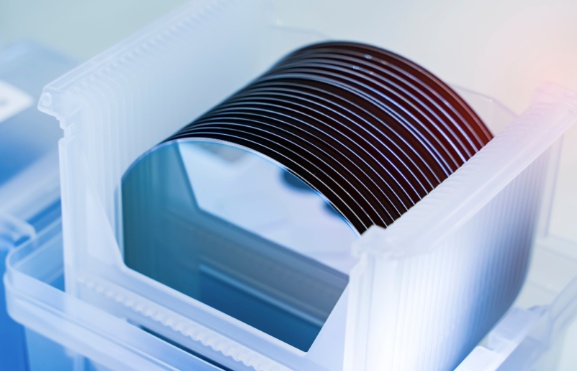
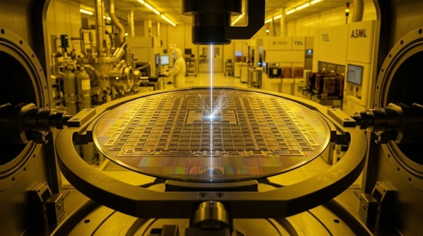
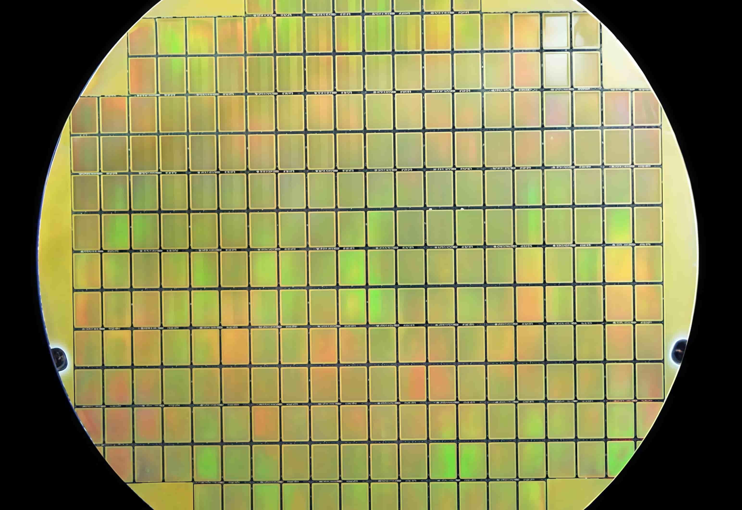
YURAY provides end-to-end OEM support—from material selection and preparation to process development, characterization, and performance testing.




Dicing
Mechanical & laser dicing
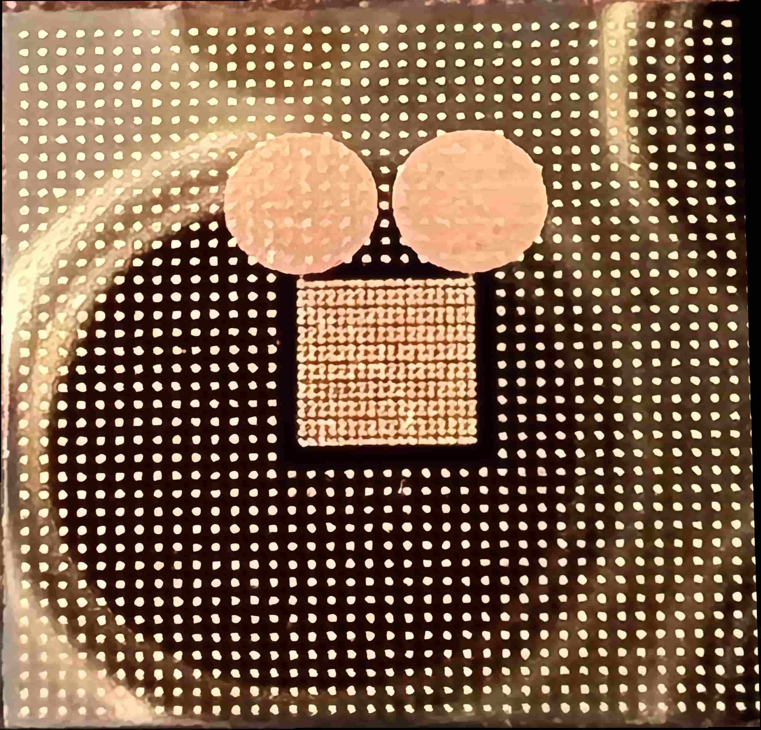
Bonding
Hybrid & anodic wafer bonding
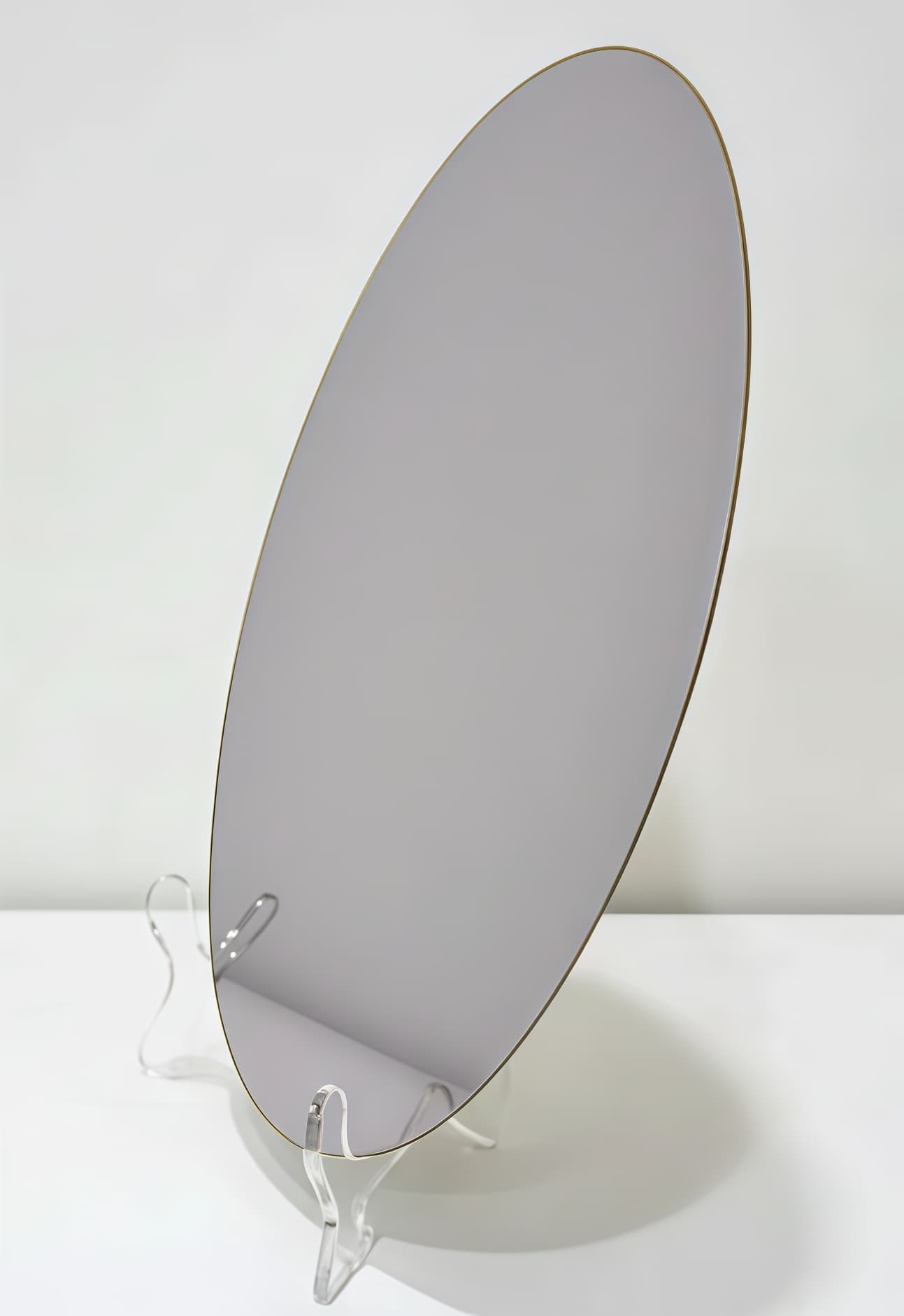
Wafer Thinning
Back-grinding & CMP planarization
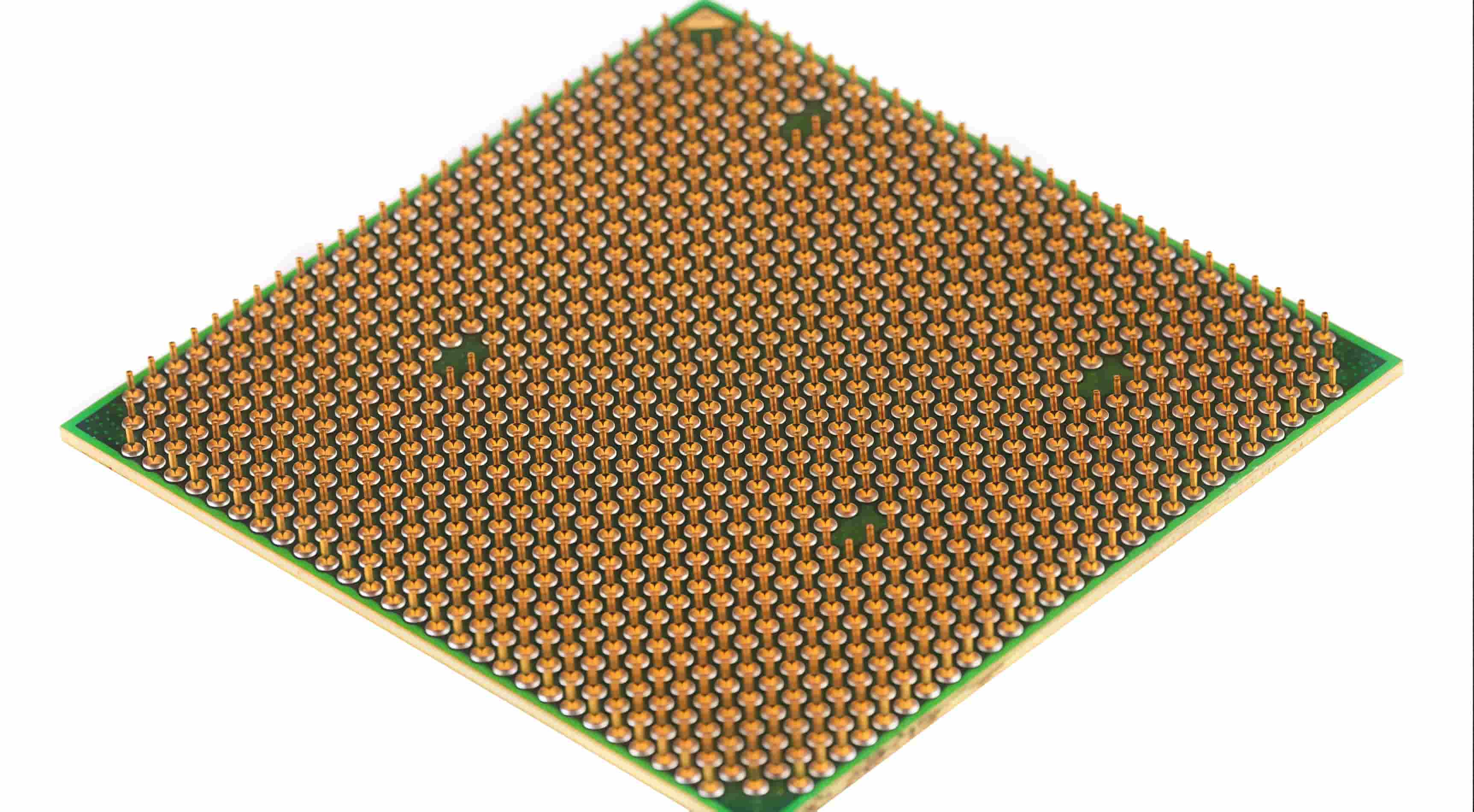
Electroplating
Cu pillar, bump & RDL plating

Etching
DRIE, ICP, RIE & metal etching
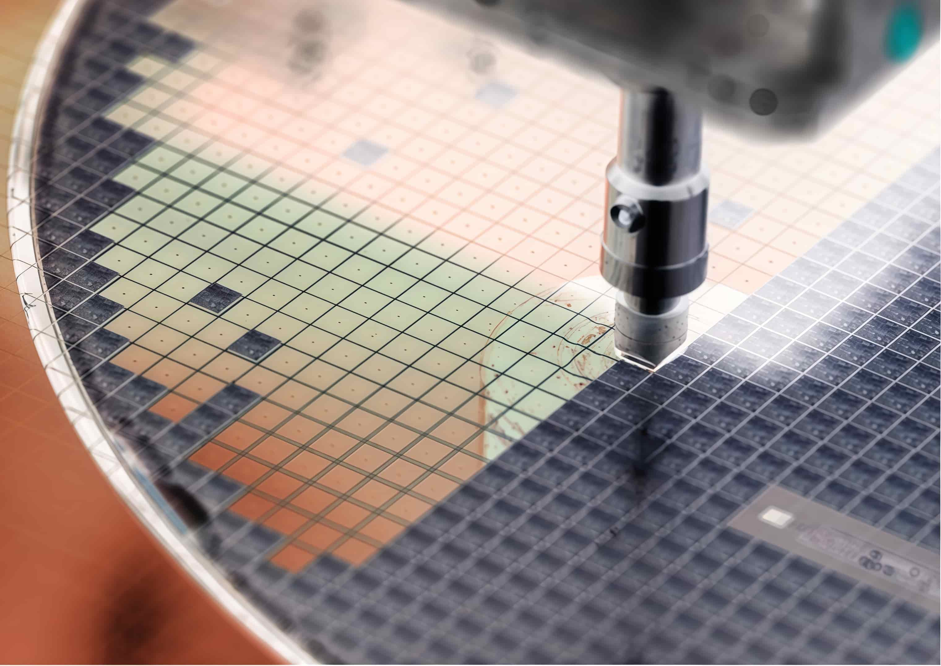
Photolithography
Contact aligner, stepper & step-and-scan
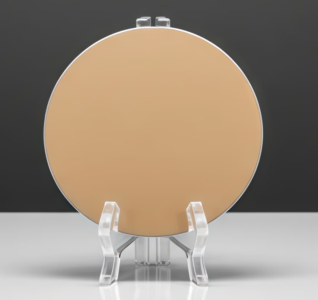
Film Deposition
PVD, CVD, ALD & thermal evaporation
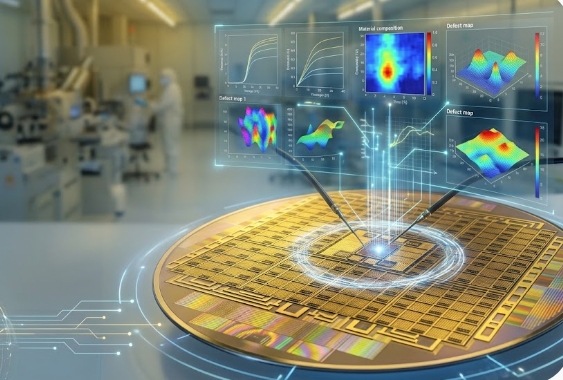
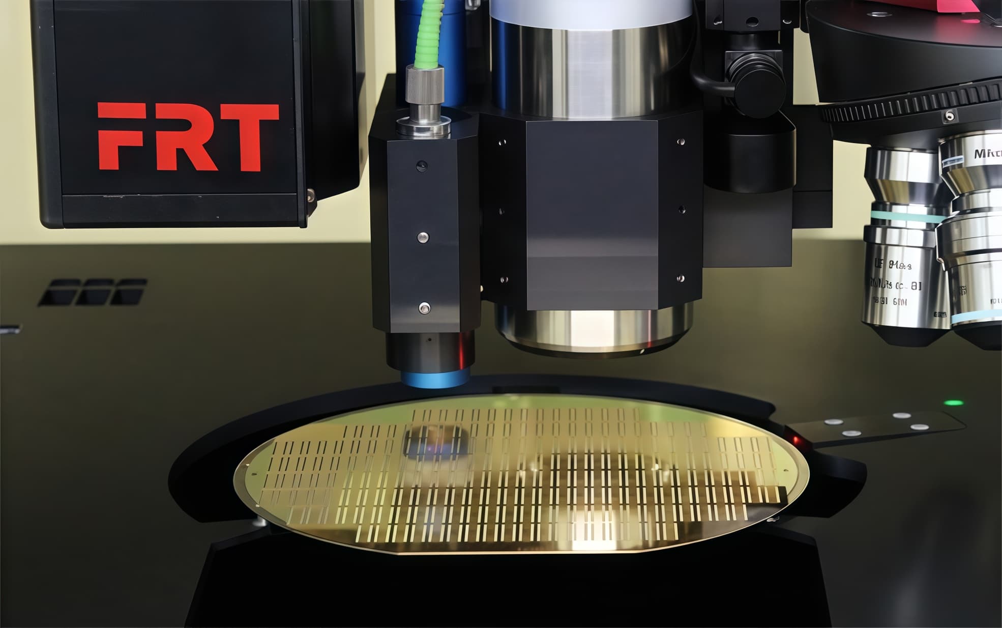
AOI
Automated optical inspection
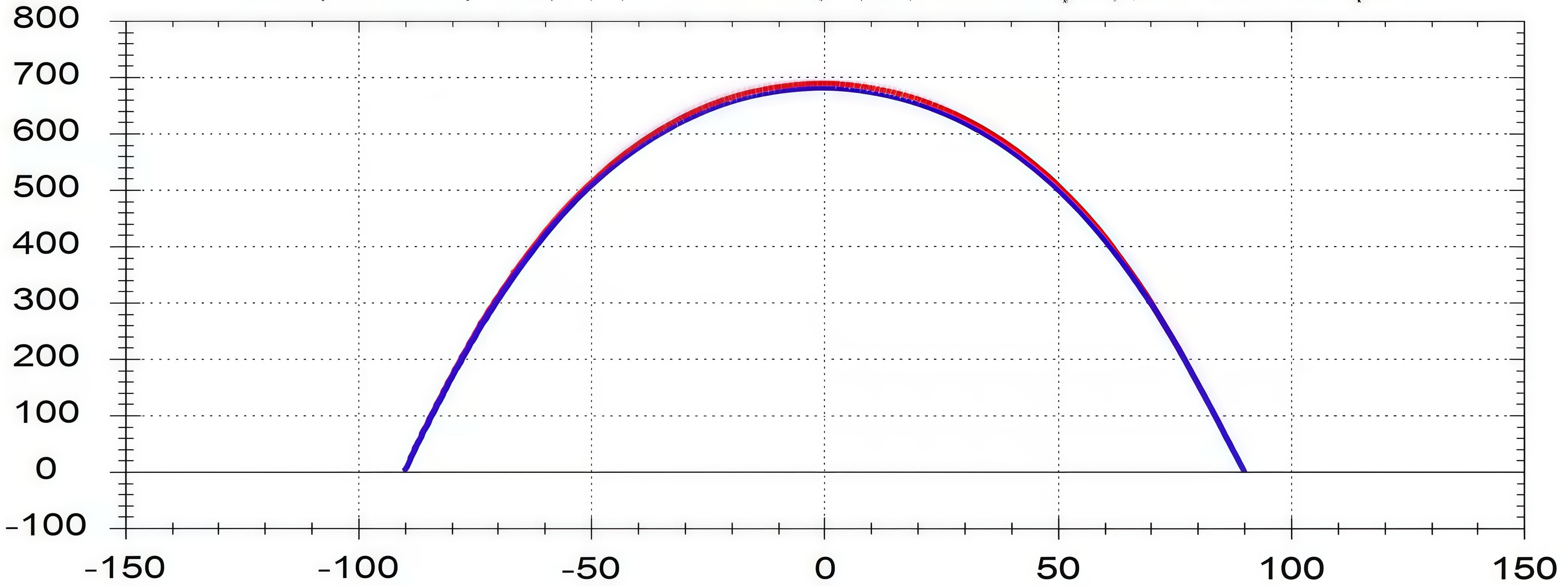
Warpage Measurement
Wafer bow & flatness metrology
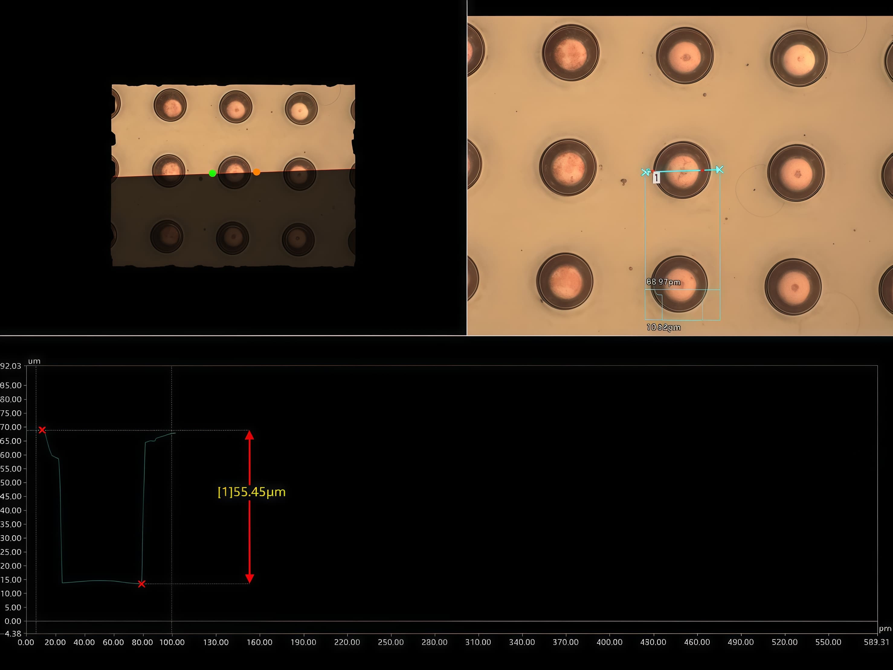
Laser Scanning Confocal Microscope
3D confocal surface profiling
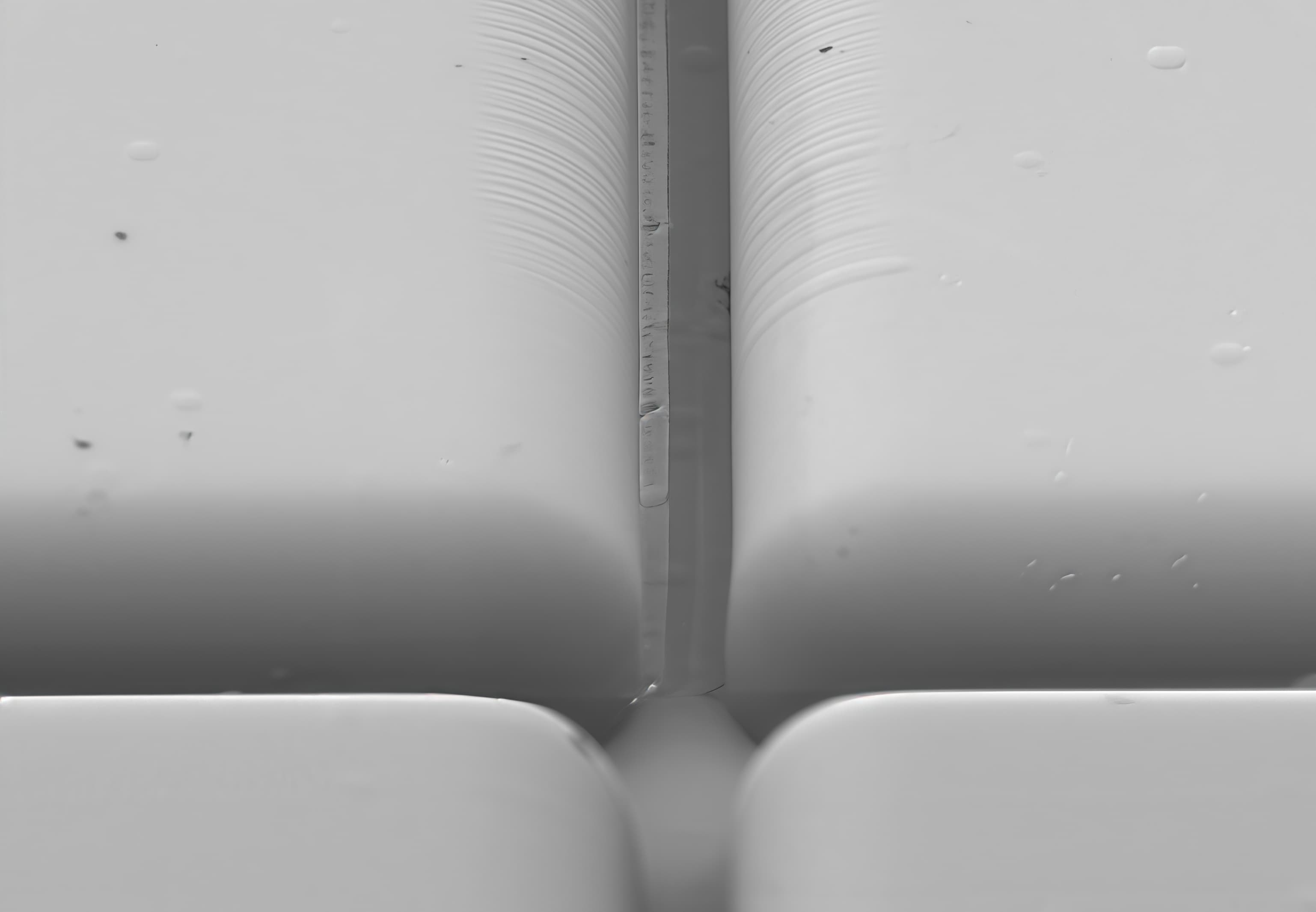
FIB
Focused ion beam cross-sectioning
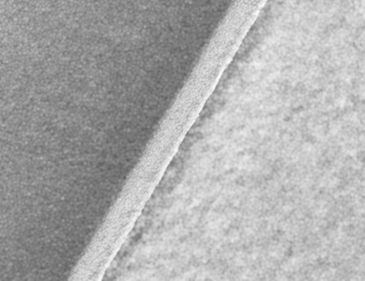
TEM
Transmission electron microscopy
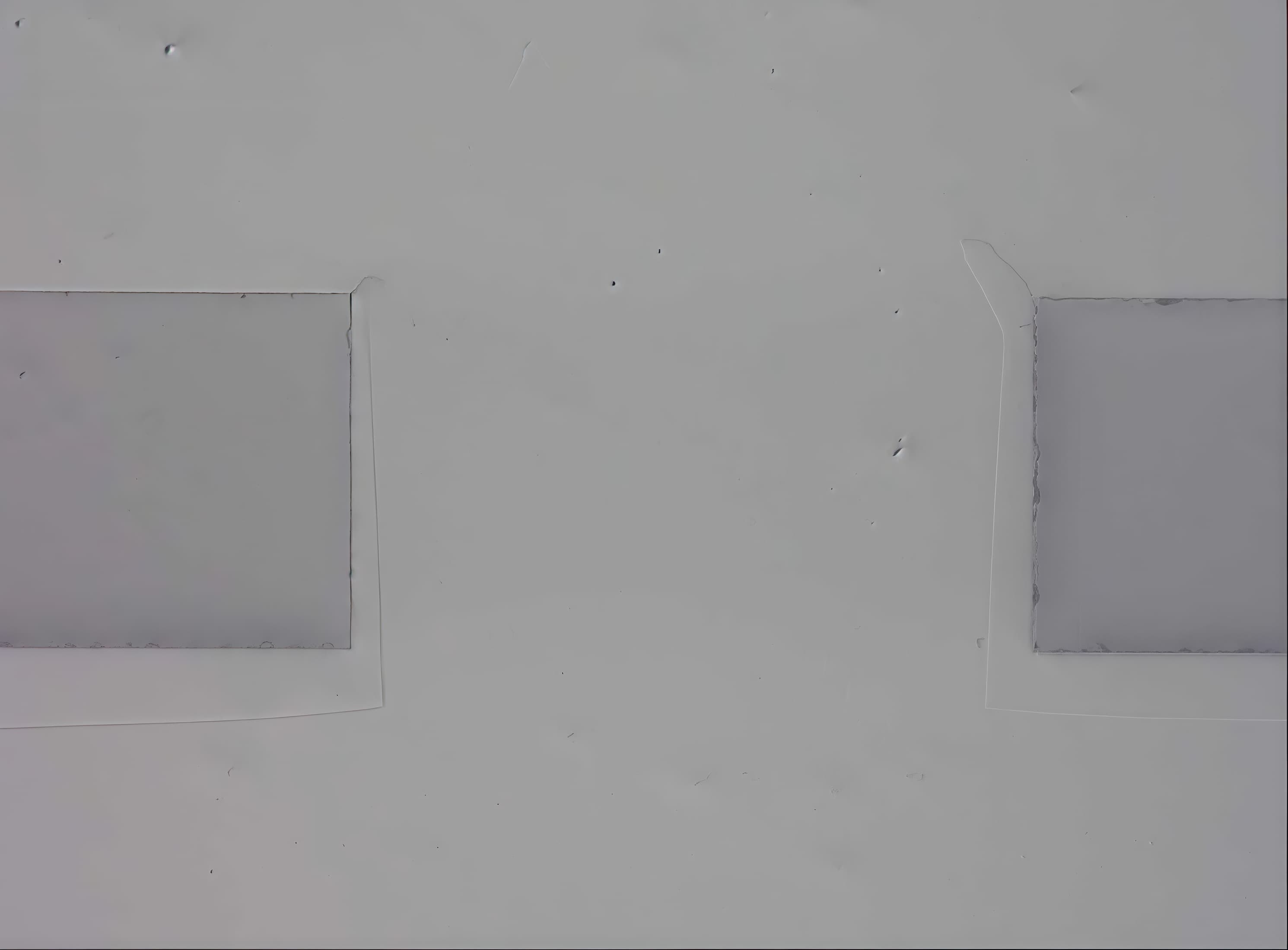
SEM
Scanning electron microscopy
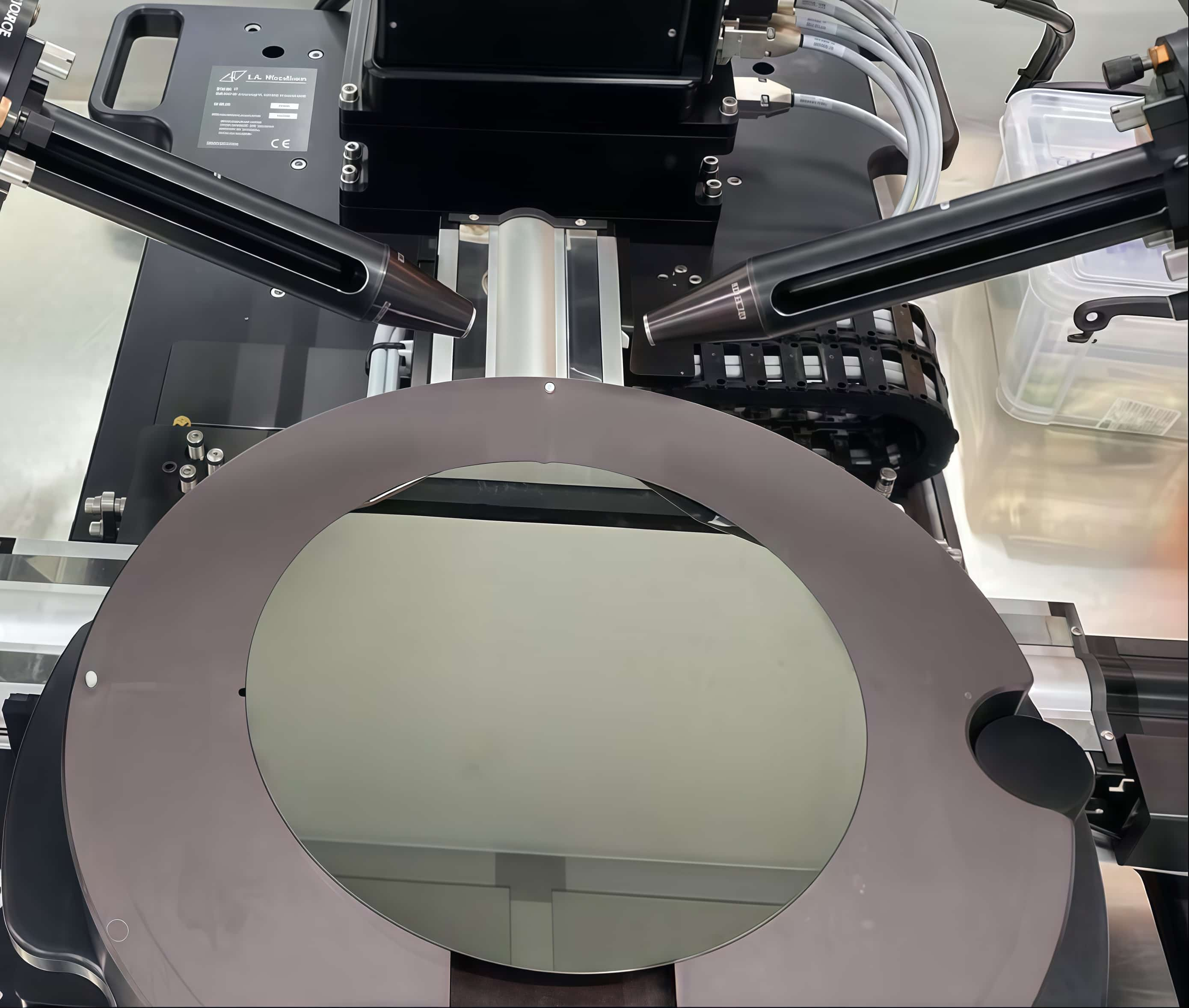
Ellipsometer
Film thickness & optical constants
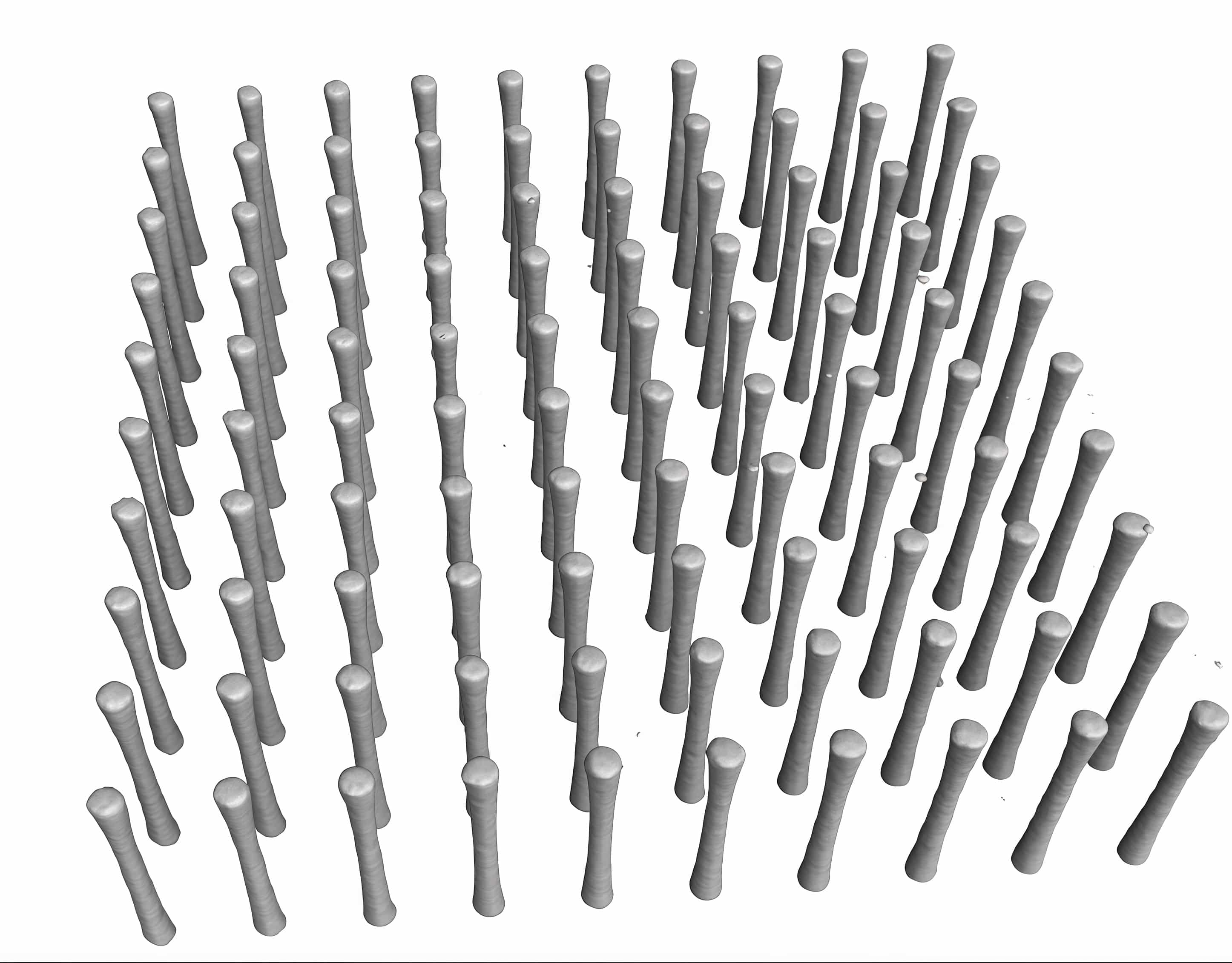
CT
Computed tomography 3D imaging
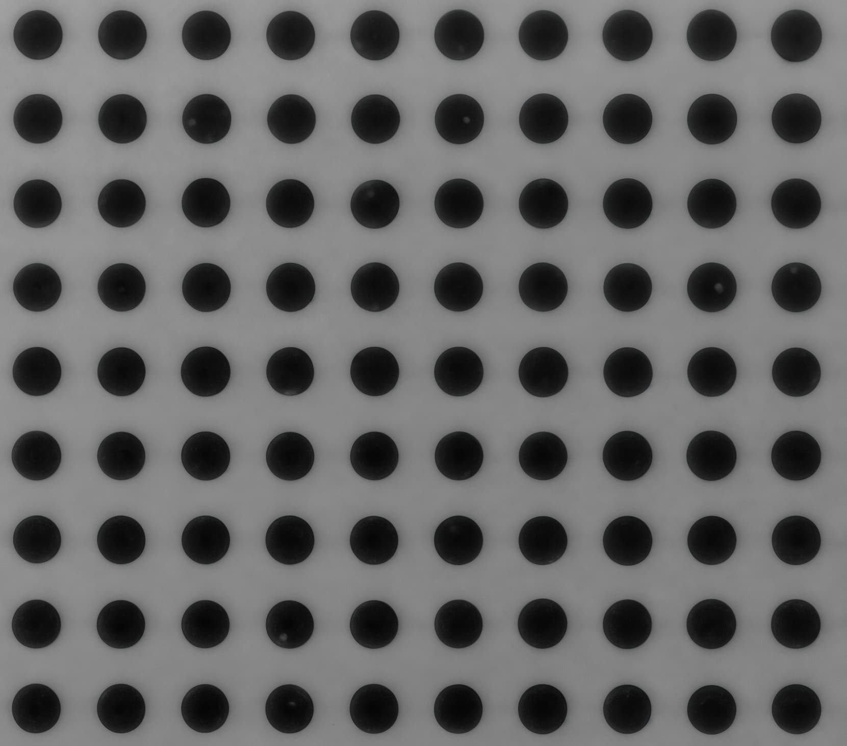
X-Ray
X-ray imaging & inspection
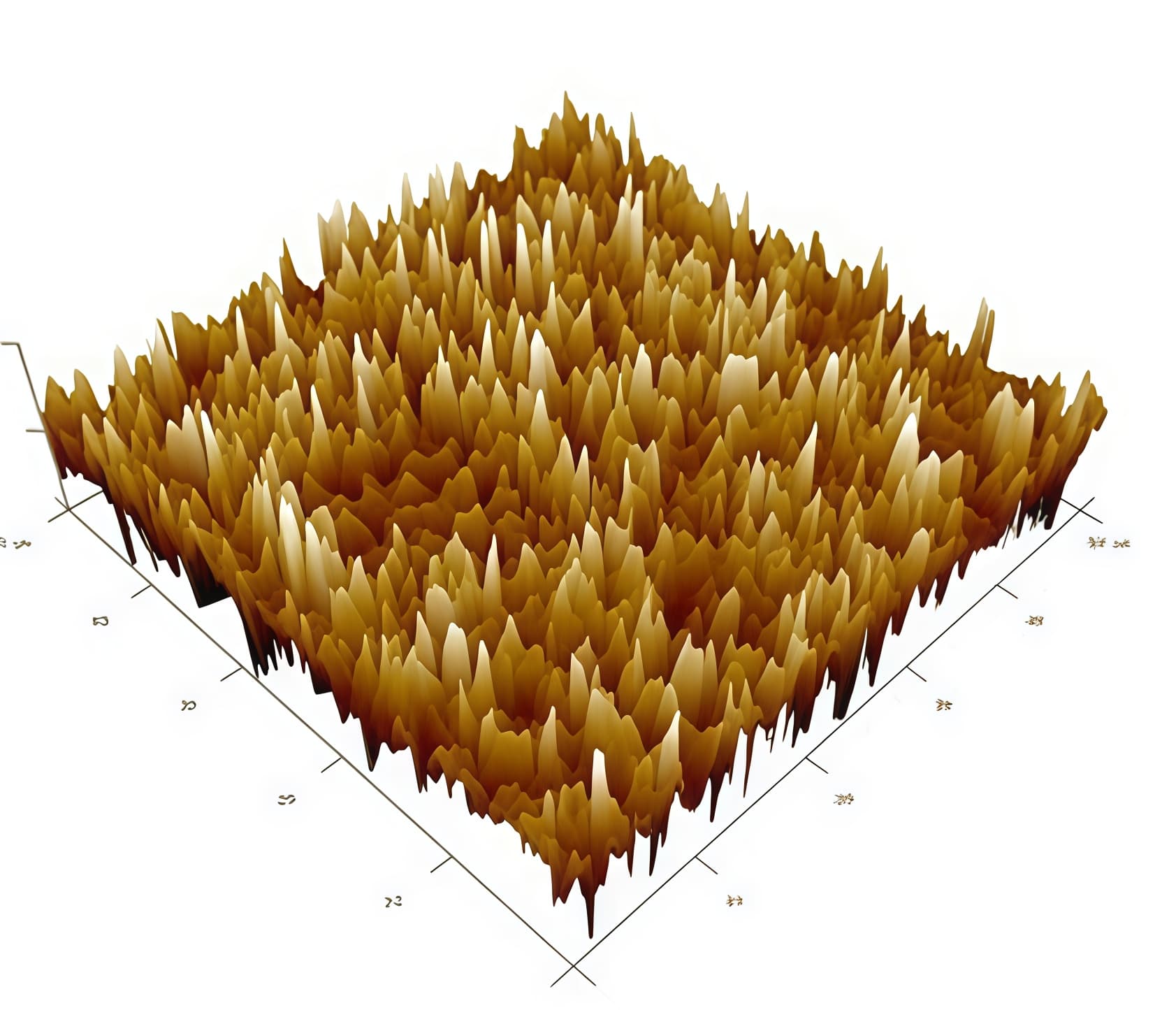
AFM
Atomic force surface topography
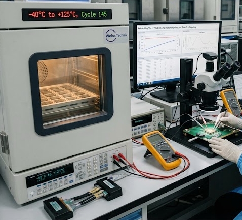

Precision Probe Testing / Precision Probe Measurement
Fine-pitch probe measurement
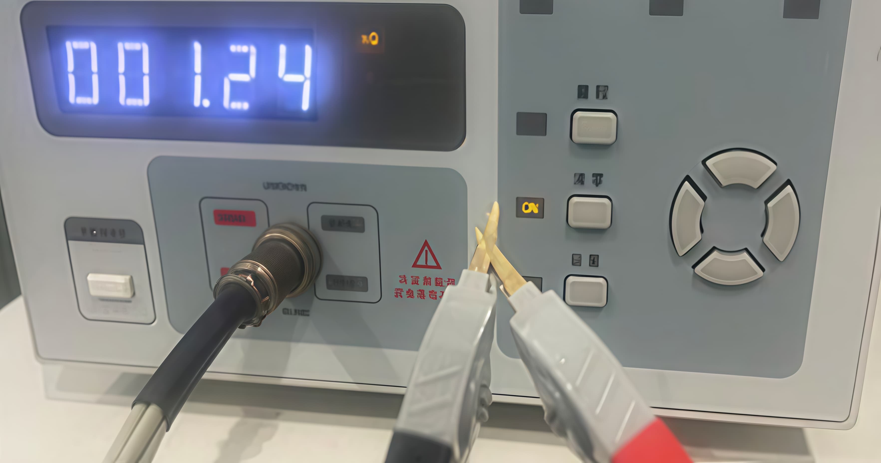
Kelvin Resistance Measurement
Low-resistance contact measurement
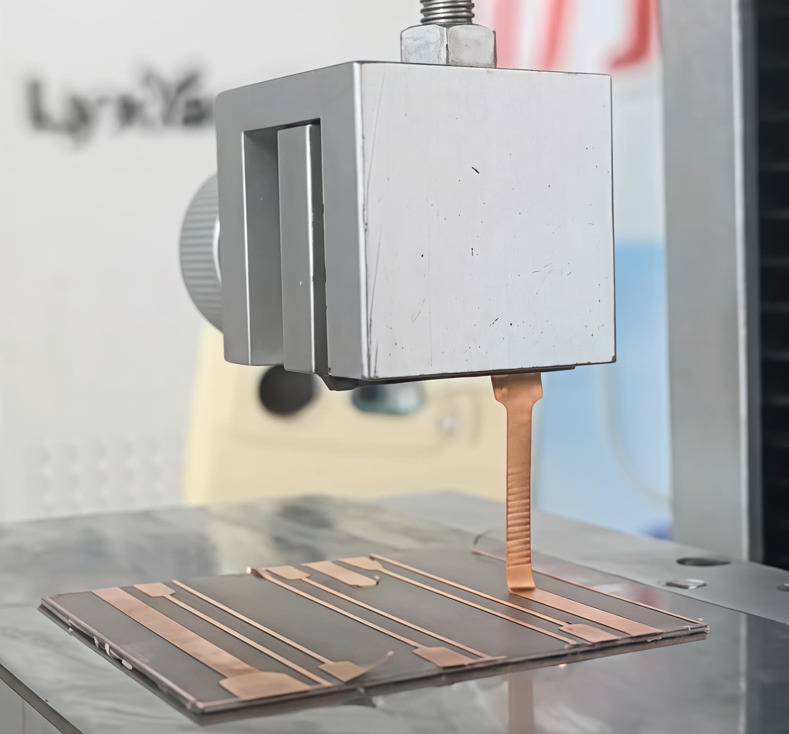
Peel Testing / Peel Strength Testing
Adhesion & peel strength
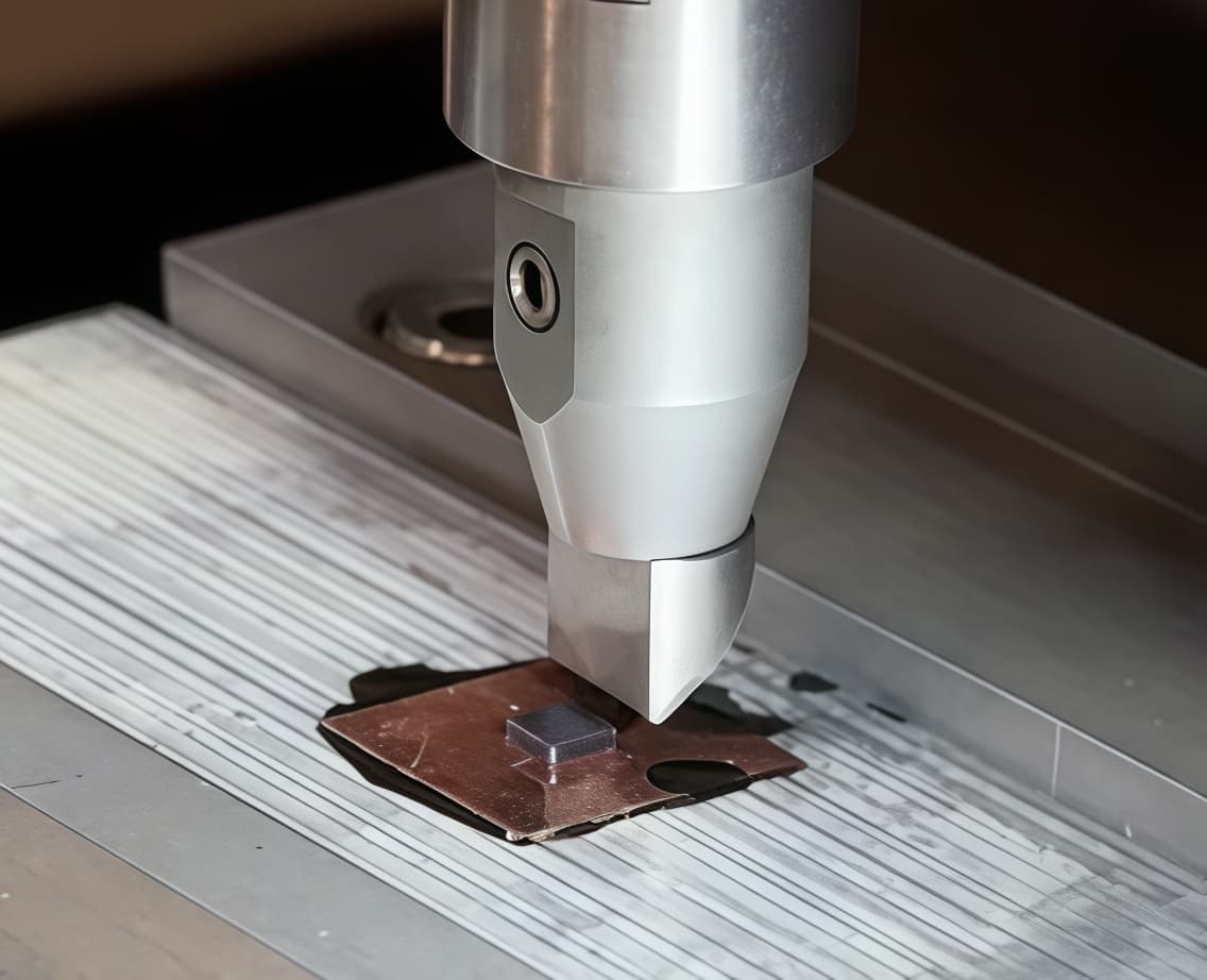
Tensile Testing / Pull Testing
Bond & joint strength measurement
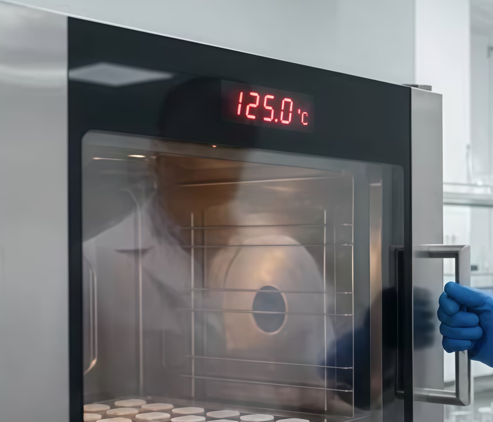
High-Temperature Testing
Thermal stability & endurance
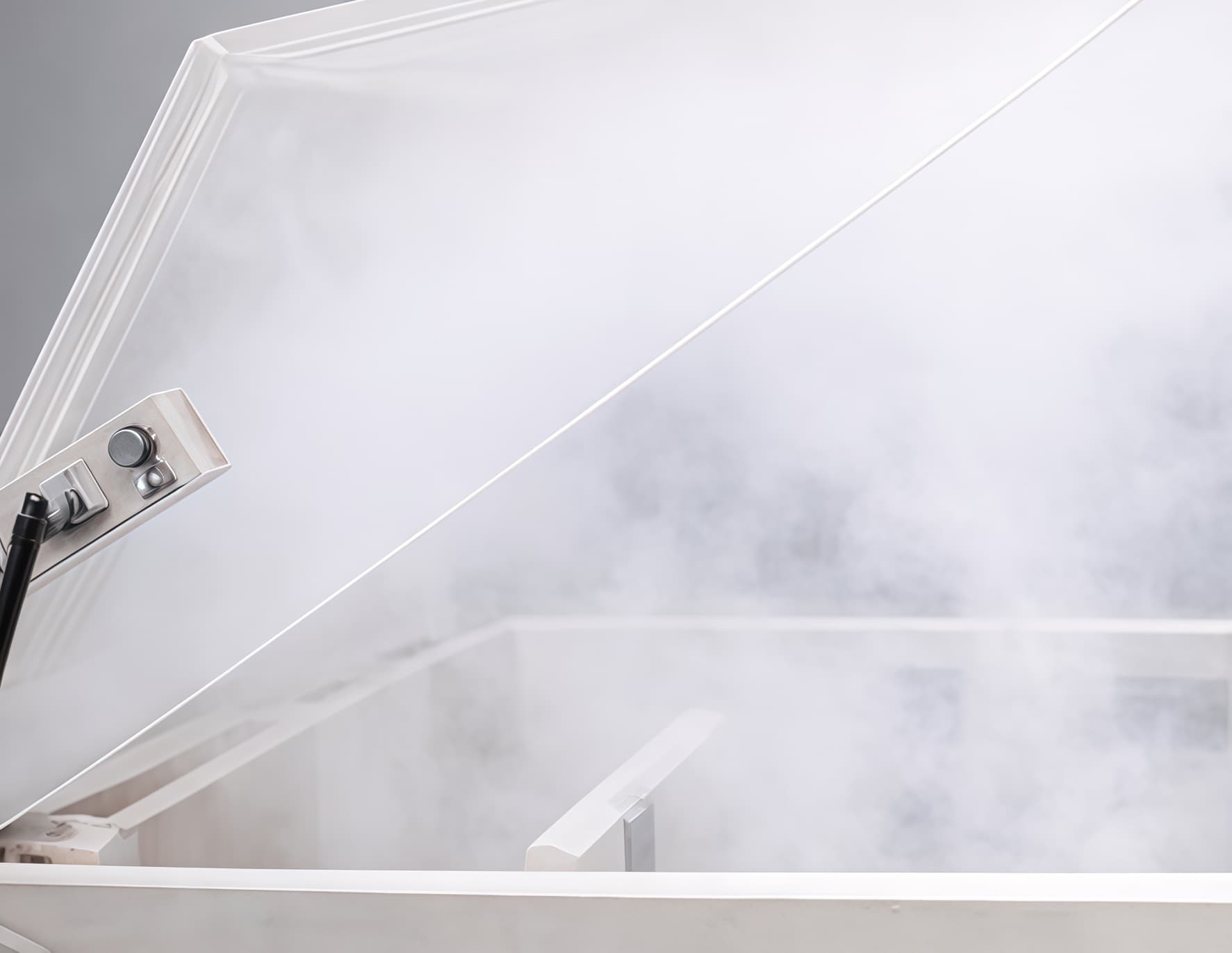
Salt Spray Testing / Salt Fog Testing
Corrosion resistance verification
Technology Roadmap
Building a progressive capability path in advanced packaging — from proven interconnect processes to next-generation glass-based and optical integration solutions.
Foundation: Flip-Chip & TSV Interposer Fabrication
Building core capabilities in Flip-chip assembly and TSV interposer manufacturing to support high-density micro-connects and 2.5D/3D advanced packaging solutions.


Expansion: TGV Technology Development
Developing through-glass via technologies, including glass via formation, metallization, and interposer integration, to enable low-loss, high-frequency, and high-performance packaging platforms.
Application: TGV Applications & CPO Integration
Extending TGV-based interposer applications across high-speed, RF, and interposer integration markets, while advancing Co-Packaged Optics (CPO) solutions for next-generation data connectivity and computing systems.

Why YURAY
More than a fabrication partner—we help transform complex technical challenges into practical, scalable solutions
End-to-End Process Chain
From substrate sourcing through deposition, lithography, etching, bonding, bumping, and full characterization — one integrated workflow, no handoffs.
R&D & Small-Batch Focus
We support research institutions, confidential R&D teams, and startups — flexible single-step services with technical support and testing reports.
Closed-Loop Quality Delivery
Every batch includes detailed test reports — SEM, AFM, X-ray, ellipsometer, thermal/mechanical/electrical characterization — before shipment.
Process Precision Guaranteed
DRIE aspect ratio up to 30:1, TSV vias as small as 3µm, CMP Ra under 1nm — qualified with SEM/CT inspection and reliability testing.
Trsusted Partners
We support research institutions, confidential R&D teams, and startups with flexible process services, technical support, characterization, and reporting.






About YURAY TECH
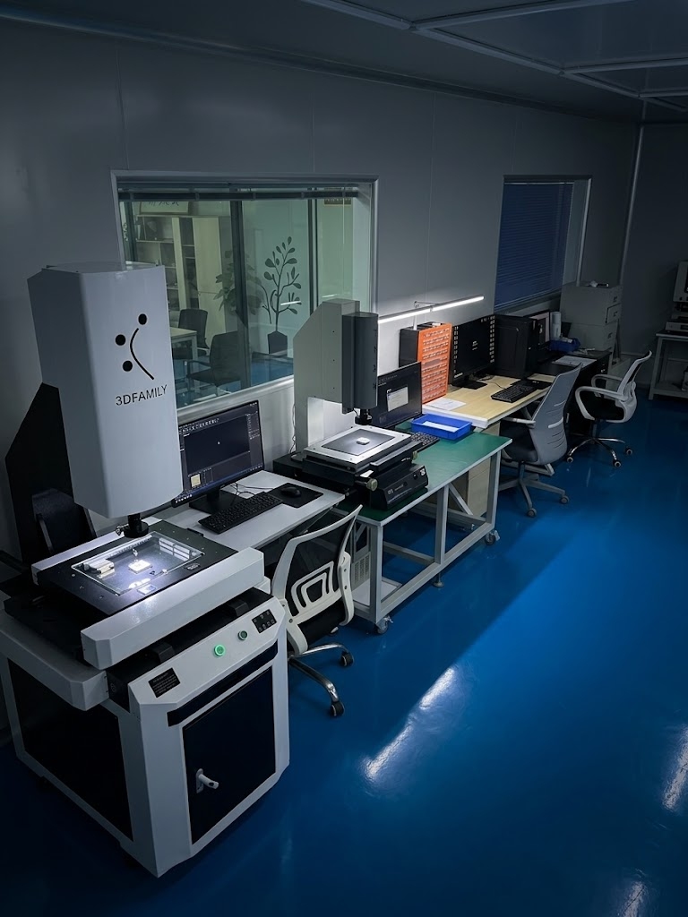
YURAY TECH is a technology-driven partner specializing in microfabrication, advanced interconnects, and semiconductor packaging.
We combine process expertise, flexible engineering support, and end-to-end manufacturing capabilities to help innovators move from concept to validated solutions
Tailored Solutions
Across the Value Chain
SOW Quantification
We meticulously analyze your Statement of Work to quantify exact project requirements and deliverables.
Process Confirmation
Our engineering team defines and validates the optimal fabrication processes for your specific needs.
Material Provision
We source and provide premium grade materials required to ensure the highest manufacturing quality.
Process Execution
Expert technicians execute precise micro and nano fabrication techniques in our state-of-the-art facility.
Characterization
We utilize advanced metrology tools to conduct rigorous physical and structural characterization of wafers.
Testing & Reporting
Comprehensive testing and detailed reporting ensure all final deliverables perfectly align with your original SOW.
Advancing TGV Glass Interposers for Next-Gen High-Bandwidth Packaging
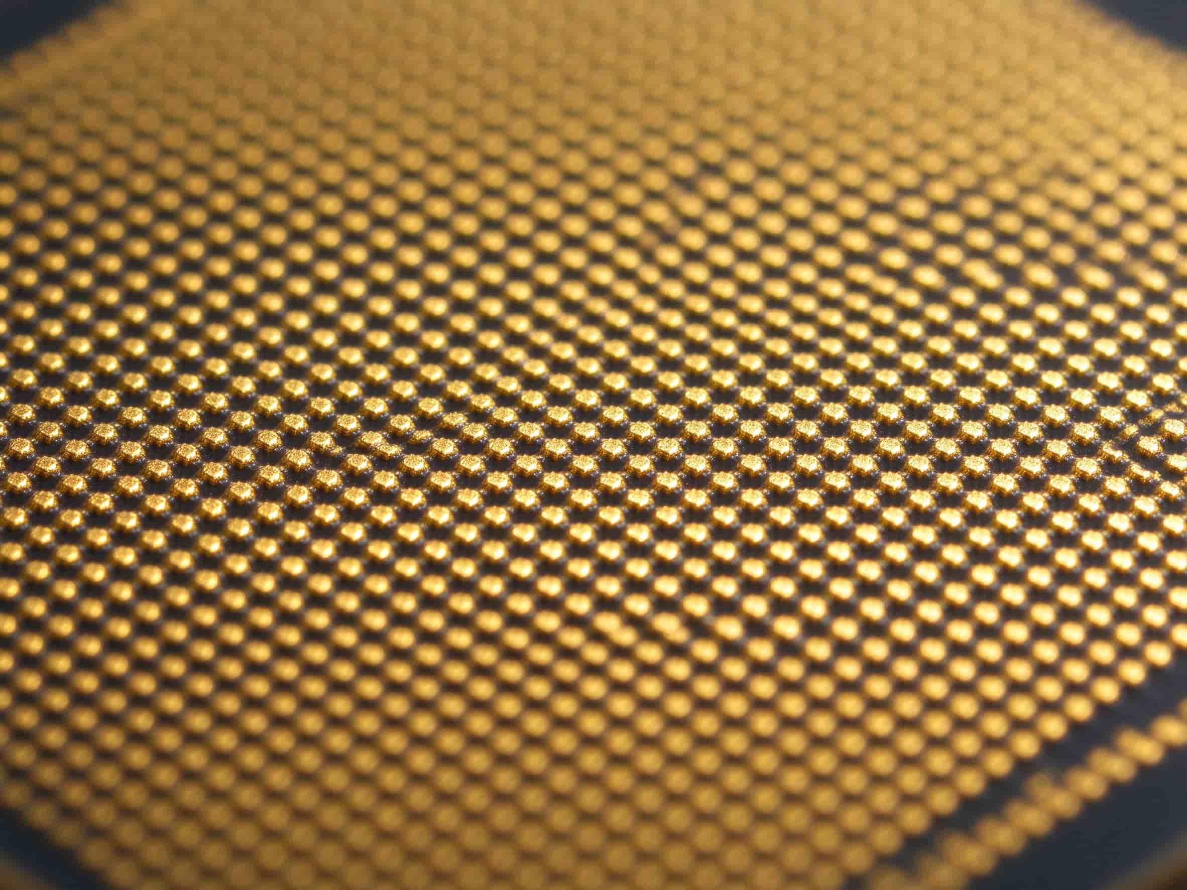
YURAY Partners with Leading Research Institute on 2.5D Interposer R&D
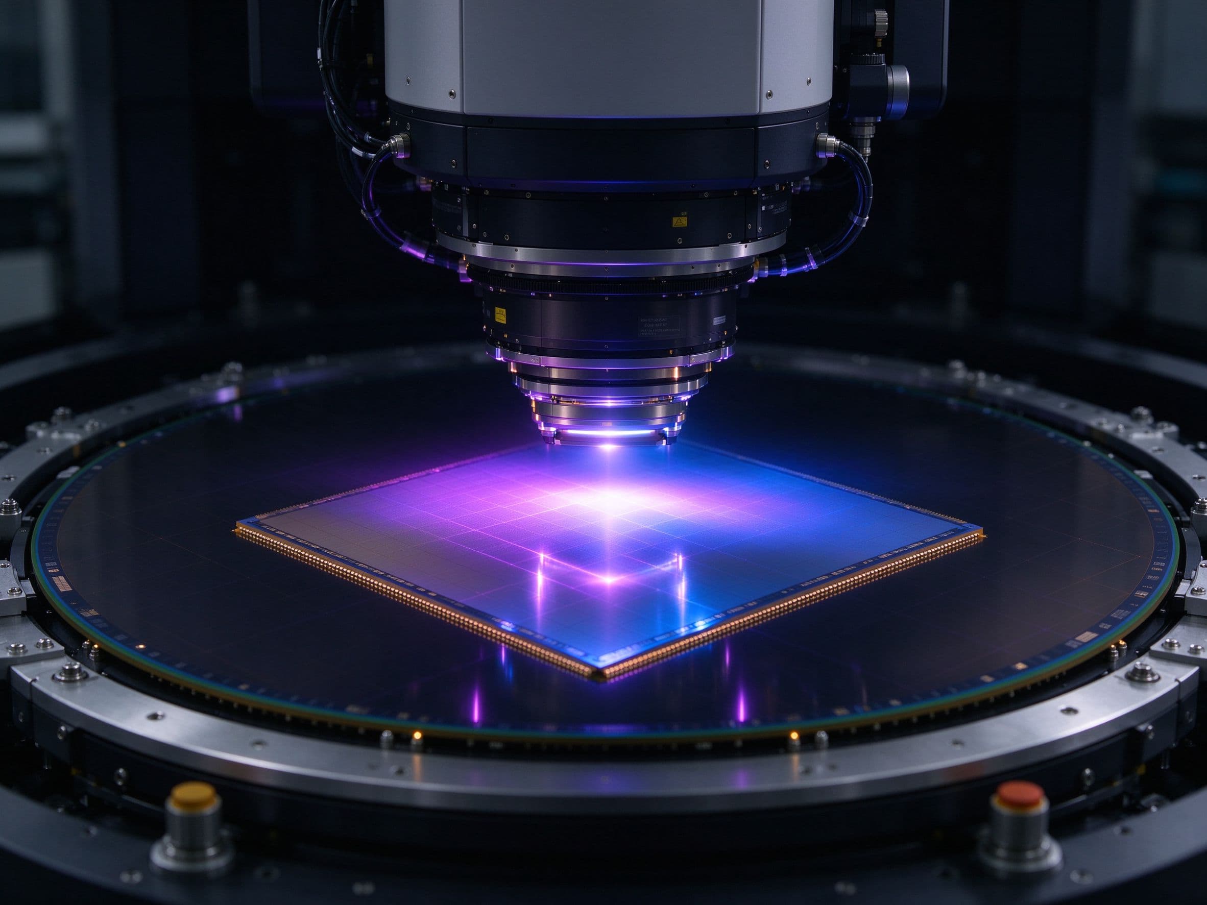
Glass Substrates for mmWave 5G/6G Front-End Modules
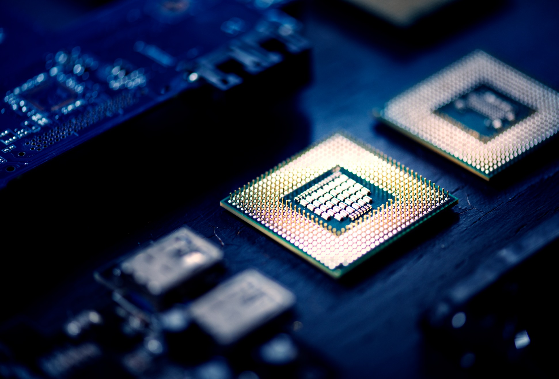
Co-Packaged Optics (CPO): The Next Frontier in Data Center Interconnects
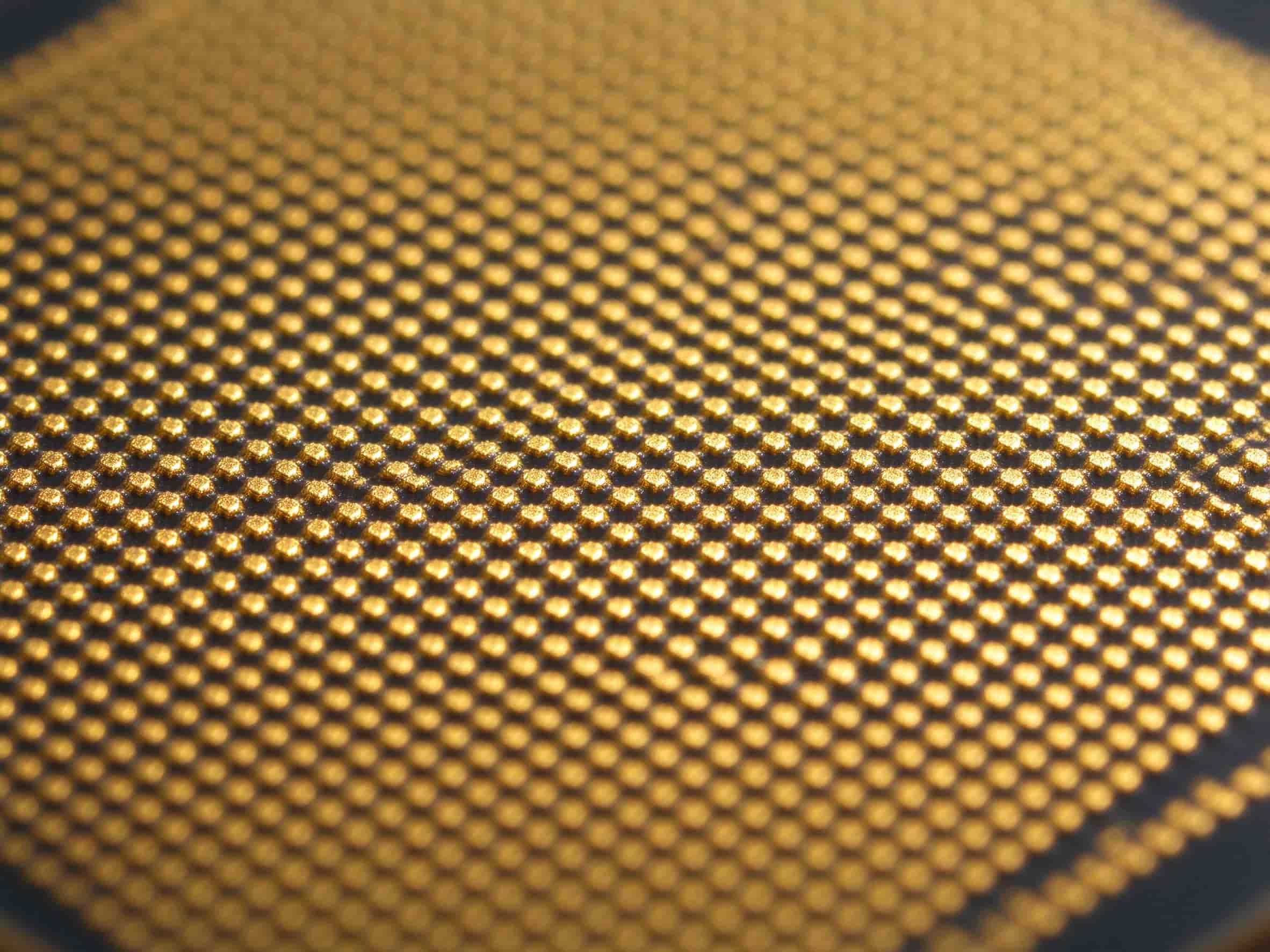
YURAY TECH Expands Metrology Lab with New AFM and SEM Capabilities
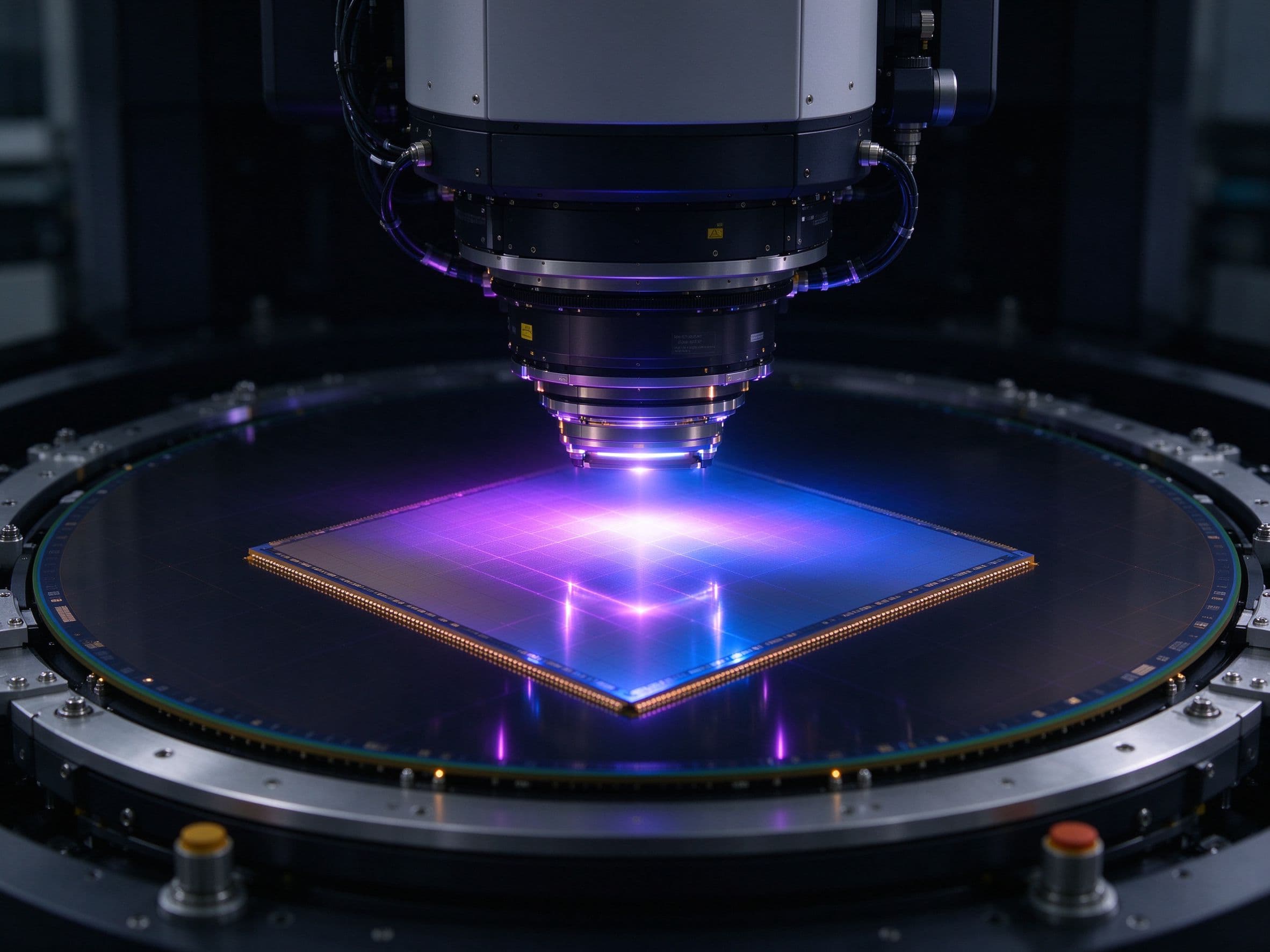
Why 3D IC Stacking Matters for AI Accelerator Roadmaps
Start Your OEM Project
with YURAY
Whether you need material evaluation, process development, prototype fabrication, characterization, or performance testing, our team is ready to discuss your requirements.